Mod-01 Lec-26 Etching and deposition (growth)
Overview of Lithography and Etching Processes
Introduction to Lithography
- Lithography is a process that transfers patterns from a mask onto wafers, essential for integrated circuit (IC) design.
- The lithography process involves two main steps: transferring the pattern onto a photoresist layer and then onto the wafer itself.
Photoresist Layer
- Photoresist is a photosensitive material that can either dissolve when exposed to light (positive photoresist) or become less soluble (negative photoresist).
- After applying the photoresist, the pattern must be transferred to the wafer through etching or growth processes.
Understanding Etching
Definition and Importance of Etching
- Etching is defined as the removal of material from the top layers of a wafer, often combined with lithography.
- There are two primary types of etching: wet etching and dry etching.
Wet Etching Process
- Wet etching uses liquid chemicals to remove material; wafers are immersed in an etchant under controlled conditions.
- For silicon etching, potassium hydroxide (KOH), typically at 30% concentration and 90°C, is commonly used.
Post-Wet Etch Procedures
- After wet etch, wafers are cleaned with distilled water to remove excess chemicals before further processing.
- Wet etch is suitable for removing large areas but may not provide precision for smaller patterns.
Key Factors Affecting Etch Rate
- Factors such as temperature, concentration of chemicals, and external agitation influence the uniformity and rate of etching.
- Initial experiments help determine optimal conditions for consistent etch rates before actual wafer processing.
Common Issues in Etching
Incomplete and Over-Eting
- Incomplete etch occurs when insufficient time or incorrect parameters prevent complete material removal.
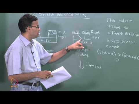
- Overetching can lead to undercutting where lateral material removal widens patterns beyond intended dimensions.
Selectivity in Wet Etchants
- Selectivity refers to how well an etchant removes one material while preserving another; KOH shows high selectivity for silicon over silicon dioxide.
Transitioning to Dry Etching
Advantages of Dry Etching
- Dry etching utilizes gases as primary mediums allowing for precise control over small features compared to wet methods.
Types of Dry Etching Techniques
- Plasma Etching:
- Plasma generation allows chemical reactions that effectively remove materials like SiO2 using fluoride gases such as CF4.
- Ion Beam Milling:
This physical removal method bombards surfaces with high-energy ions but lacks selectivity due to its purely physical nature.
- Reactive Ion Etching:
- Combines both plasma chemistry and ion beam techniques for enhanced directional control during material removal.
Growth Processes Overview
Deposition vs. Growth
- Unlike etched layers which involve removing materials, deposition adds new materials without consuming underlying silicon.
Techniques for Deposited Layers
- Physical Vapor Deposition (PVD):
- Typically used for metallic layers; details will be covered in future discussions on metallization processes.
- Chemical Vapor Deposition (CVD):
- Used extensively for growing dielectric materials like silicon dioxide or nitride through gas-phase reactions.
- Atomic Layer Deposition (ALD):
- A precise method growing materials one atomic layer at a time by alternating gas introductions leading to monolayer formation.
- Molecular Beam Epitaxy (MBE):
- Utilizes molecular beams for highly controlled growth of thin epitaxial layers with excellent composition accuracy.
Turn any video into a summary like this
YouTube links, meetings, lectures. With transcripts, search, and chat.