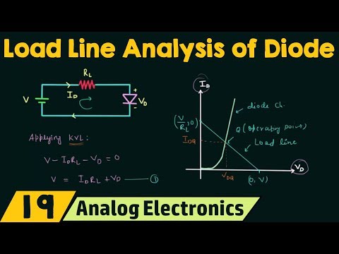
Load Line Analysis of Diode
Load Line Analysis of PN Junction Diode
Introduction to Load Line Analysis
- The load line analysis is used for graphical representation in non-linear electronic circuits, such as diodes and transistors.
- Non-linear circuits do not adhere to Ohm's law, resulting in non-linear voltage-current (VI) characteristics.
Understanding the Circuit Components
- In the circuit, the diode voltage is denoted as V_D , with R_L representing load resistance and V as the external voltage source.
- Kirchhoff's Voltage Law (KVL) can be applied: V - I_D R_L - V_D = 0 .
Deriving Key Equations
- Rearranging KVL gives us Equation 1: V = I_D R_L + V_D .
- When V_D = 0 , the diode current ( I_D ) can be calculated as I_D = V/R_L .
Identifying Points on the Load Line
- Two critical points are established:
- Point A at coordinates (V/R_L, 0)
- Point B at coordinates (0, V)
- The intersection of these points forms a straight line known as the load line, which intersects with the diode characteristics at a point called the Q point or operating point.
Analyzing Slope and Changes in Resistance
- The slope of the load line can be derived from Equation 1. Dividing both sides by R_L :
- Results in a linear equation format where slope ( m ) is equal to -1/R_L .
- Changing load resistance ( R_L ) affects both slope and Q point position; thus altering circuit behavior significantly.